
Researchers develop a 3D transistor stacking process that boosts performance in flexible and wearable electronics without overheating.

Flexible displays, wearable sensors and many IoT devices need more transistors per unit area. But the current technology, Vertical stacking, can raise density, but it faces two practical problems: rough interfaces that accumulate defects across layers, and thermal-process limits that prevent use of standard high-temperature steps. These problems reduce device yield and circuit reliability.
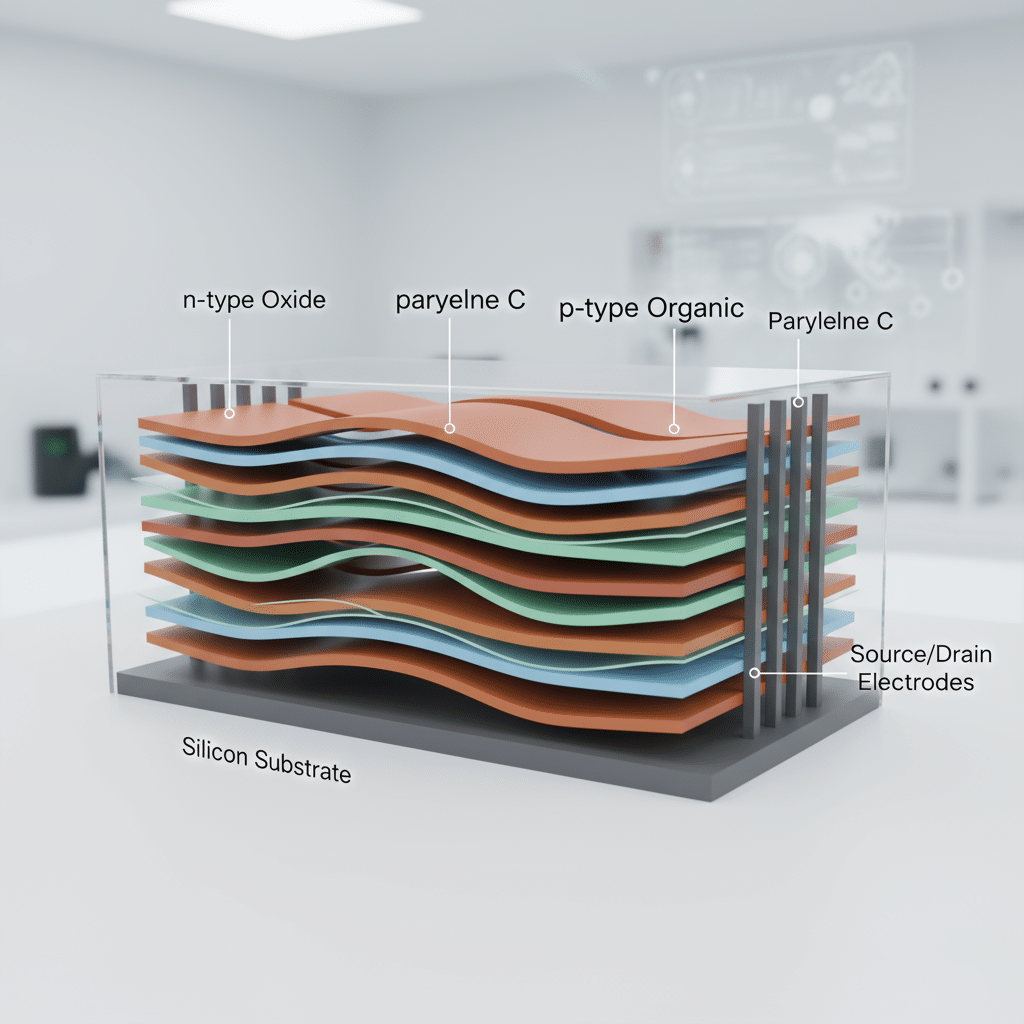
The researchers developes a new way to stack transistors vertically without these problem. The process alternates n-type oxide transistors and p-type organic transistors across six stacks. The full structure comprises 41 layers.
Each layer is built at low temperature and separated by a thin a thin film coating to improve the capabilities of leading-edge technologies called parylene C film, which keeps the surfaces smooth and prevents electrical leakage between layers. The new design reduces wiring distance and improves power efficiency while keeping manufacturing compatible with large-area, flexible substrates.
The team fabricates and measures 600 transistors to check uniformity and reproducibility. Balanced electron and hole transport yields comparable saturation currents across stacks, which supports CMOS-style logic.
The researchers integrate oxide and organic devices into 300 hybrid inverters. The inverters show a maximum gain of about 94.8 V/V and a minimum measured peak power of 0.47 µW, indicating low-power switching that matters for battery-powered and energy-harvesting systems.
The group also builds four-stack NAND and NOR gates and validates correct logic behaviour under test conditions. Reliability testing shows device characteristics begin to degrade above 50 °C, reflecting the low thermal budget of the process.
Post-fabrication oxygen plasma and 200 °C anneal steps improve interface quality and reduce subthreshold swing. The work establishes a scalable route for denser, low-power, large-area circuits. The next technical steps are improving thermal robustness and refining interfacial smoothness to meet industrial operating ranges.
The research was published in Nature Electronics.